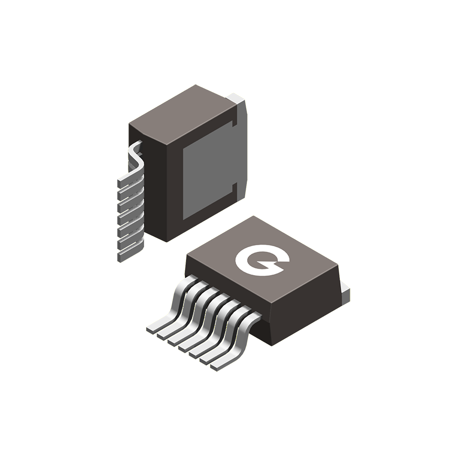
TO-263-7
Performance Features
- Multi-Pin Parallel Design: Multiple source and drain pins are paralleled within the 7-pin layout, reducing connection resistance and inductance.
- Excellent Thermal Performance: The bottom pad is directly soldered to the PCB, providing an efficient thermal conduction path.
- Low Package Parasitic Parameters: Ideal for high-frequency, high-current switching applications.
- High Current Carrying Capability: Significantly enhances both continuous current and pulsed current handling capacity.
Core Advantages
- Reduced Conduction Losses: The multi-pin parallel design effectively lowers the total connection resistance, minimizing I²R losses.
- Enhanced High-Frequency Performance: Low parasitic inductance reduces voltage overshoot and oscillation, enabling higher frequency operation.
- Improved Heat Dissipation: The large-area bottom pad provides an efficient heat dissipation channel, lowering junction temperature.
- High Power Density Solution: Combines low losses with high current density to achieve high power density designs.
Key Applications
- Energy Storage Systems (ESS): Power Conversion Systems (PCS) or high-voltage bidirectional DC-DC converters.
- Power Tools: Motor drives for high-power cordless drills, chainsaws, and other equipment.
- Battery Management Systems (BMS): High-current charge/discharge protection circuits.
- Industrial Automation: High-power servo drives and Uninterruptible Power Supplies (UPS).
相关产品
