
Dual-Side Cooling Clip Packaging for Low-Impedance Power MOSFETs: Applications & Future Trends
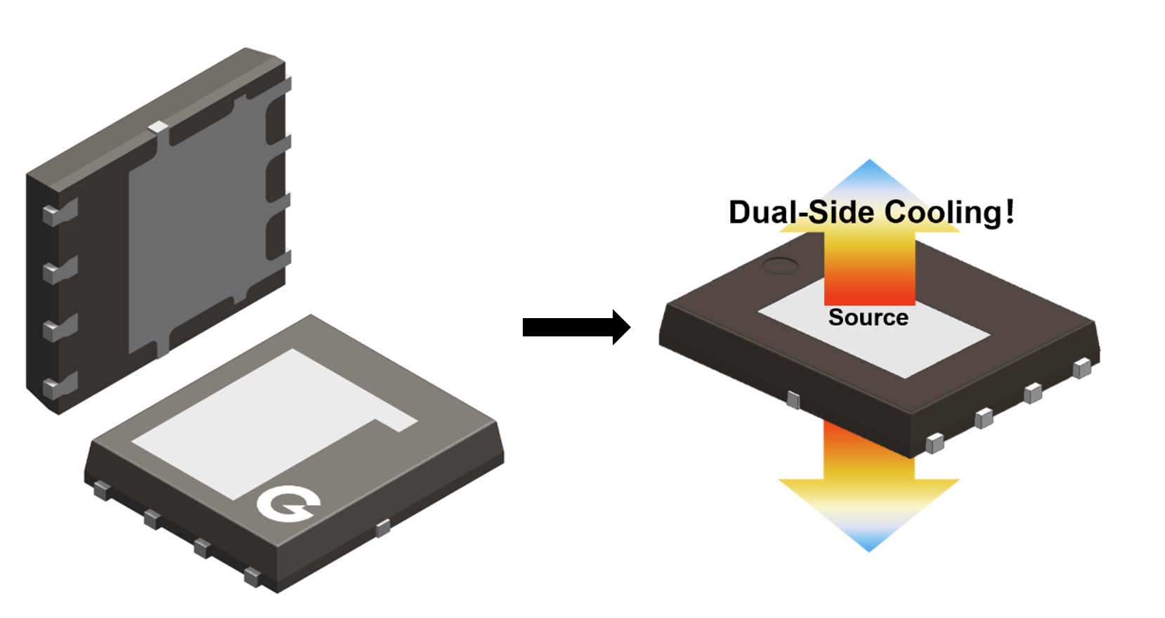
- From “Single‑Side Warfare” to “Double‑Side Clamping”: Technical Essence
1.1 Thermal Challenges of Conventional Packages
Traditional PDFN5×6‑8L packages dissipate heat only through the bottom PCB, resulting in a single heat‑flow path. When currents exceed 200 A, junction temperature rises rapidly, leading to:
- RDS(on)increases by 40 % with temperature, causing a sharp drop in efficiency;
- Junction‑to‑ambient thermal resistance Rθ JA typically exceeds 30 °C/W, making heat dissipation a clear bottleneck;
- Power cycling lifetime falls below 100 k cycles, limiting reliability.
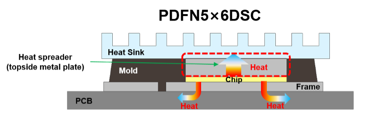
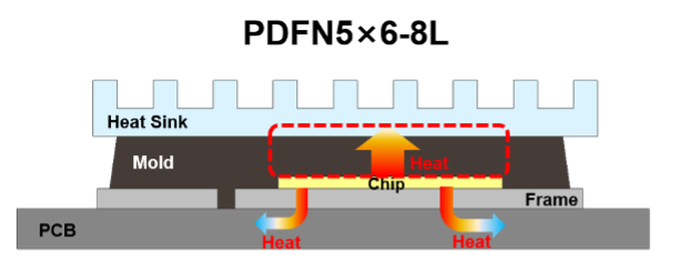
1.2 Architectural Revolution of Dual‑Side Cooling
Galaxy Microelectronics’ PDFN5×6DSC (Dual‑Side Cooling) package achieves dual‑side heat extraction through three major innovations:
- Clip copper replacing aluminium ribbon:A 460 µm thick copper clip is soldered directly onto the top of the chip, serving as the primary heat‑conduction path.
- Exposed top metal pad:Forms dual top‑and‑bottom heat paths together with the bottom drain pad.
- Insulating thermal pad:The top side is connected to a heatsink via an insulating sheet, providing electrical isolation while maintaining high thermal conductivity.
Measured data: The junction‑to‑case thermal resistance of the TBLS009N04THSC is only 0.85 °C/W, which is 20 % lower than that of conventional single‑side cooling packages. At a high current of 100 A, the temperature rise of the device is reduced by 5–10 °C.
- Overwhelming Performance: Six Core Advantages of Dual‑Side Cooling
Based on measured comparative data (TBLS009N04THSC vs. conventional single‑side package):
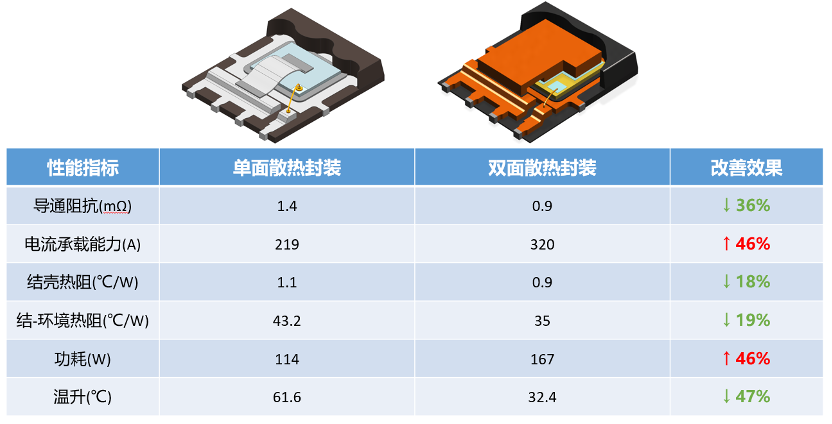
2.1 Ultimate Thermal Dissipation Capability
Key principle: Heat is simultaneously conducted from both the top and bottom surfaces of the chip, effectively doubling the cross‑sectional area of the heat‑flow path.
Case study: In a 24 V BMS system, 28 TBLS009N04THSC devices are paralleled. Dual‑side cooling reduces the maximum system temperature from 136 °C to 125 °C, significantly lowering the MOSFET failure rate.
2.2 Sustained Ultra‑Low Impedance
The Clip technology itself pushes RDS(on) down to 0.6 mΩ (typ.), and the excellent heat dissipation ensures that this low impedance is maintained even at high temperatures:
- At 25 °C: 0.6 mΩ
- At 175 °C: increases to only 1.1 mΩ (temperature coefficient of only 1.8×, far lower than the 2–3× typical of aluminium‑ribbon designs).
2.3 High Reliability Design
- Power cycling lifetime:Dual‑side cooling reduces thermo‑mechanical stress; measured endurance exceeds 500 k cycles (vs. <100 k cycles for conventional packages).
- Short‑circuit ruggedness:When 28 paralleled TBLS009N04THSC devices are subjected to a 2400 A short‑circuit surge, the junction temperature remains within the safe operating area after a 300 ms pulse, whereas the single‑side package has already failed.
- Application Scenarios: Industries Transformed by Dual‑Side Cooling
3.1 Battery Management Systems (BMS) – The Core Battlefield
Pain point: In EV BMS, short‑circuit events can subject the system to instantaneous currents exceeding 3000 A, leading to severe temperature rise and demanding high reliability.
TBLS009N04THSC solution:
- 28–36 devices paralleled for charge/discharge protection;
- 2400 A overcurrent test: temperature rise limited to 125 °C (vs. 136 °C for competing solutions);
- Short‑circuit withstand time of 0.3 s, 50 % longer than competitors;
- Top heatsink can be directly connected to the battery housing, eliminating the need for an additional heat sink.
Customer validation: In a BMS solution from a leading automotive manufacturer, adoption of dual‑side cooling reduced the number of MOSFETs by 20 % while lowering overall system cost by 15 %.
3.2 AI Server Power Supplies – A Revolution in Power Density
Challenge: GPU power modules demand current densities exceeding 150 A/in², making thermal management impossible with conventional packages.
Value of dual‑side cooling:
- A top‑side heatsink directly attached to the MOSFET cuts thermal resistance by half;
- Efficiency improvement of 1.5 % translates to annual energy savings of thousands of kilowatt‑hours per rack.
3.3 Traction Inverters – High‑Reliability Assurance
Requirement: Automotive main drives undergo frequent start‑stop cycles, requiring power cycling capability >300 k cycles.
Technical fit: The combination of clip bonding and dual‑side cooling reduces solder‑joint stress by 60 % and delivers power cycling lifetime exceeding 500 k cycles, fully meeting AEC‑Q101 standards.
- Challenges and the Future: Technology Roadmap
4.1 Current Challenges
- Cost pressure:The addition of top‑side cooling processes makes dual‑side cooling 15–20 % more expensive than single‑side packages.
- Design complexity: PCBs must consider electrical isolation and thermal design on both top and bottom sides, demanding more from engineers.
- Lack of standardisation: Top‑side pad dimensions and insulation voltage ratings have not yet been unified across the industry.
4.2 Galaxy Microelectronics’ Solutions
- Process optimisation:Clip soldering yield has been improved to 99.5 %, reducing manufacturing costs.
- Design tools: We provide complete electrical and thermal simulation models.
- Customer support:Free samples and technical support are offered to ensure that dual‑side cooling delivers its full performance potential.
- Technology Outlook: The Pursuit of Thermal Excellence Never Ends
Dual‑side cooling with clip technology is not merely a packaging enhancement—it represents a paradigm shift in power semiconductor design philosophy. With its three pillars of dual heat paths, ultra‑low impedance, and high reliability, it underpins the next generation of power electronic systems.
Galaxy Microelectronics’ vision: By the end of 2026, we aim to achieve cumulative sales of over one million TBLS009N04THSC units, while developing even lower‑impedance derivatives such as the TBLS006N04THSC, continuing to lead the industry.
For engineers, the window of opportunity to transition from single‑side to dual‑side cooling is wide open. In high‑performance applications such as BMS, servers, and traction drives, dual‑side cooling is no longer an option—it is an engineering imperative. For the industry, as standardisation matures and costs decline, dual‑side cooling will become the new normal for power MOSFETs, just as flip‑chip packaging did for logic devices.
Dual‑side cooling is here—and the future is bright!