New Benchmark in Advanced Protection: Snap-Back ESD Diodes – Building Robust Defenses for Electronic Devices

Electronic devices face persistent risks of electrostatic discharge (ESD) throughout daily production and operation. As an advanced protection solution, Snap-Back ESD protection diodes deliver superior performance and have become the preferred protection device for high-speed data interfaces, automotive electronics, mobile devices and other applications.

What Is Snap-Back Technology?

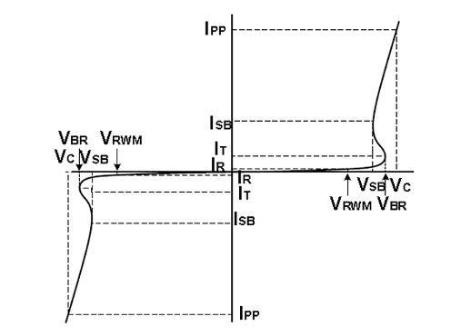
Snap-Back technology enables a highly efficient ESD protection mechanism. When the applied voltage exceeds the specific trigger voltage, the device rapidly turns on and diverts transient high current to ground, protecting precision downstream components and circuits. For conventional ESD protection devices, voltage rises nearly linearly in proportion to increasing IPP (Peak Pulse Current). In contrast, Snap-Back devices exhibit negative differential resistance after triggering: voltage drops as current increases. Thanks to this characteristic, Snap-Back devices maintain a lower clamping voltage than traditional ESD diodes under identical IPP while shunting larger currents, delivering outstanding protection performance.

V-I Characteristic Curve of Snap-Back ESD Diode

Latch-Up Effect

Under normal operating conditions, the device automatically switches off and reverts to a high-impedance state once the current through the device falls below the holding current ISB. However, latch-up will occur if the supply voltage of the circuit system exceeds the holding voltage and the on-state current remains higher than ISB. Even after the external ESD event disappears, the device cannot turn off and stays in a low-impedance, high-current conducting state. This causes voltage drop on protected downstream circuits, potentially resulting in system malfunction. Furthermore, sustained high current through the ESD protection device may lead to permanent damage. Therefore, during device selection, engineers should prioritize ESD protection devices with holding voltage higher than the system normal operating voltage. In areas highly susceptible to latch-up, devices with strong Snap-Back characteristics should be avoided to mitigate latch-up risks.

Chip Structure of Snap-Back Devices – SCR

What Is the SCR Structure?

As circuits grow increasingly sensitive to parasitic effects, the drawbacks of traditional GGNMOS structures become more prominent. SCR (Silicon-Controlled Rectifier) has emerged as a promising ESD protection device. The SCR structure forms a four-layer PNPN stack consisting of parasitic diodes, an N-well and P-substrate, creating a parasitic silicon-controlled rectifier. When the ESD voltage exceeds the trigger threshold, the internal positive feedback loop (simultaneous turn-on of parasitic NPN and PNP transistors) activates, switching the device rapidly into a low-impedance conducting state to divert ESD current. The chip structure and equivalent circuit of our low-capacitance bidirectional SCR-based ESD diode are shown below. Compared with conventional PN-junction ESD diodes, it achieves lower clamping voltage and smaller junction capacitance.
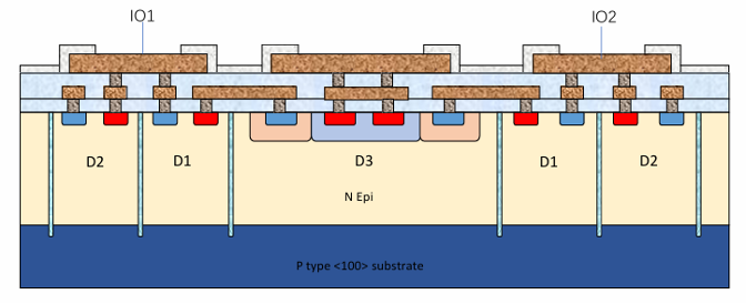
Chip Structure of Low-Capacitance Bidirectional SCR ESD Device

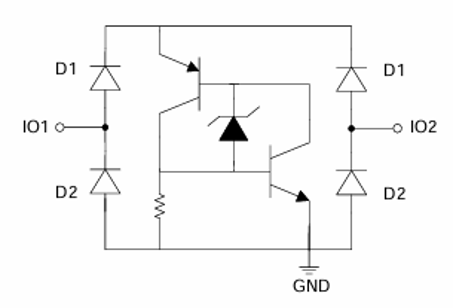
Equivalent Circuit of Low-Capacitance Bidirectional SCR ESD Device

Galaxy Microelectronics Snap-Back ESD Diode Recommendations

To meet the rising demand for enhanced port protection in consumer electronics such as smartphones and laptops, Galaxy Microelectronics leverages years of profound technical accumulation in high-performance circuit protection to launch a new generation of ESD protection devices adopting SCR process with Snap-Back characteristics.

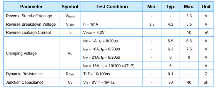
13.3V High IPP Soft Snap-Back ESD Device – ESDSSB3V3BLP3

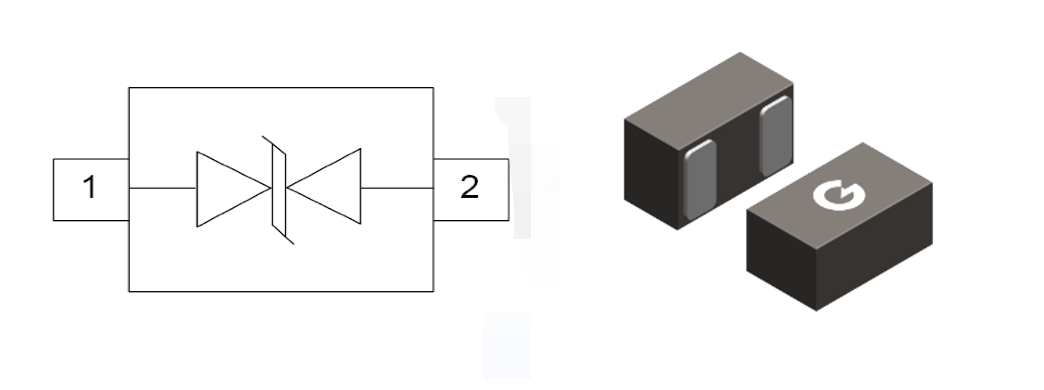
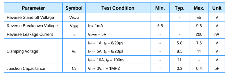
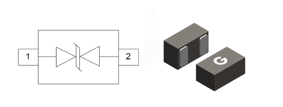
ESDSSB3V3BLP3 is a single-channel bidirectional protection device built on advanced monolithic silicon technology. It features a low trigger voltage of 4.3 V, low clamping voltage of 8 V, ultra-fast response time and ultra-low dynamic resistance, making it an ideal protection solution for voltage-sensitive data and power supply lines. Housed in an ultra-compact lead-free 0201 package (0.6×0.3 mm, DFN0603-2L), the device combines miniature form factor with robust ESD surge protection capability. It is well suited for smartphones, digital cameras, audio players and a wide range of portable devices.

Parameter Table of ESDSSB3V3BLP3

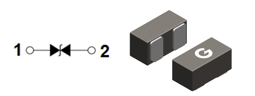
Schematic Diagram and Package Outline of ESDSSB3V3BLP3 (DFN0603-2L)

2 3.3V Ultra-Low Capacitance Soft Snap-Back ESD Device – ESDSSB3V3X3BL

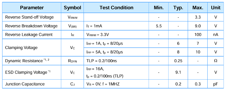
ESDSSB3V3X3BL is a 3.3 V single-channel bidirectional protection diode with ultra-low junction capacitance of 0.2 pF, low clamping voltage of 8 V and excellent dynamic resistance (0.25 Ω). It provides distortion-free protection for high-speed data interfaces. The device protects high-speed ports including USB 3.0, HDMI and DisplayPort in portable electronics such as smartphones, tablets and notebooks, ensuring signal integrity and improving system reliability.

Parameter Table of ESDSSB3V3X3BL

Schematic Diagram and Package Outline of ESDSSB3V3X3BL (DFN1006-2)

35V 4-Channel Low-Capacitance ESD Array – ESDSSB5V0X1BG4

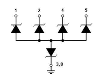
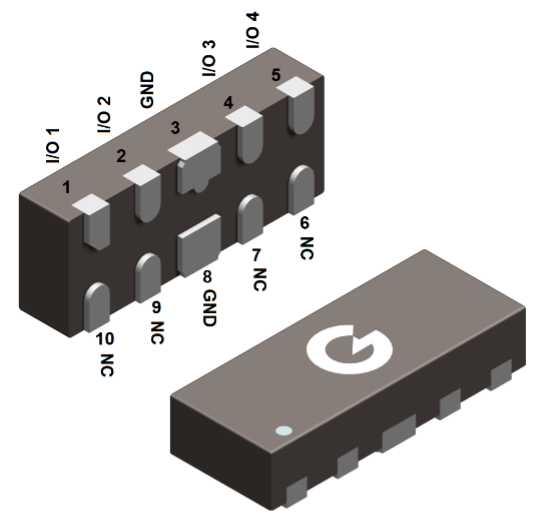
Featuring four-channel integration and excellent electrical performance, this ESD protection array delivers an efficient solution for compact multi-interface designs in modern portable devices. Packaged in miniaturized DFN2510-10L, it integrates four independent protection channels within a single chip, greatly improving PCB space utilization. With 0.3 pF junction capacitance and low clamping characteristics, it offers synchronous protection for multiple high-speed data interfaces including USB 3.0, HDMI 2.0 and Type-C. It is ideal for space-constrained portable electronic products such as smartphones and tablets.

Parameter Table of ESDSSB5V0X1BG4

ESDSSB5V0X1BG4电路图及封装图(DFN2510-10L)

424V Ultra-Low Capacitance Soft Snap-Back Device – TESDSSB24VX5BL

With a rated operating voltage of 24 V and ultra-low junction capacitance below 0.1 pF, TESDSSB24VX5BL easily withstands voltage fluctuations in vehicle power systems while introducing negligible loss to high-frequency signals to preserve signal integrity. It is applicable to automotive antenna interfaces and IoT antenna ports, and delivers superior protection for high-speed buses such as Automotive Ethernet and Camera Link.

Schematic Diagram and Package Outline of TESDSSB24VX5BL (DFN1006-2)

These product series integrate comprehensive advantages including compact packaging, low clamping voltage and low junction capacitance. Compared with traditional ESD devices, they provide more reliable transient overvoltage protection on high-speed interfaces such as USB. Their structural design ensures outstanding ESD withstand capability without compromising signal integrity. They help end-device manufacturers strengthen interface reliability and improve overall user experience.